We are building a custom asynchronous signal processor from scratch and taking it all the way to manufactured silicon. Total cost to get chips in hand: roughly $15,000. No commercial EDA licenses. No six-figure tool subscriptions. Every tool in our flow is free and open source.
Five years ago, this was not possible. The EDA tools didn't exist, the PDK wasn't open, and there was no accessible path from a Verilog file to a packaged chip. Today, the entire flow is available to anyone with a Linux machine and the willingness to learn it.
This post is a map of that flow—every tool, what it does, and where it fits. In the coming weeks, we'll go deeper into each stage and share how we adapted these tools for our fully asynchronous, clockless design.
The Tools
Yosys — Synthesis. Yosys reads your Verilog RTL and converts it into a gate-level netlist mapped to a target cell library. It is the front end of the entire flow. You hand it behavioral Verilog and it hands back a netlist of AND gates, OR gates, flip-flops, and buffers from the SKY130 standard cell library. It handles technology mapping, optimization, and generates the netlist that feeds into place and route.
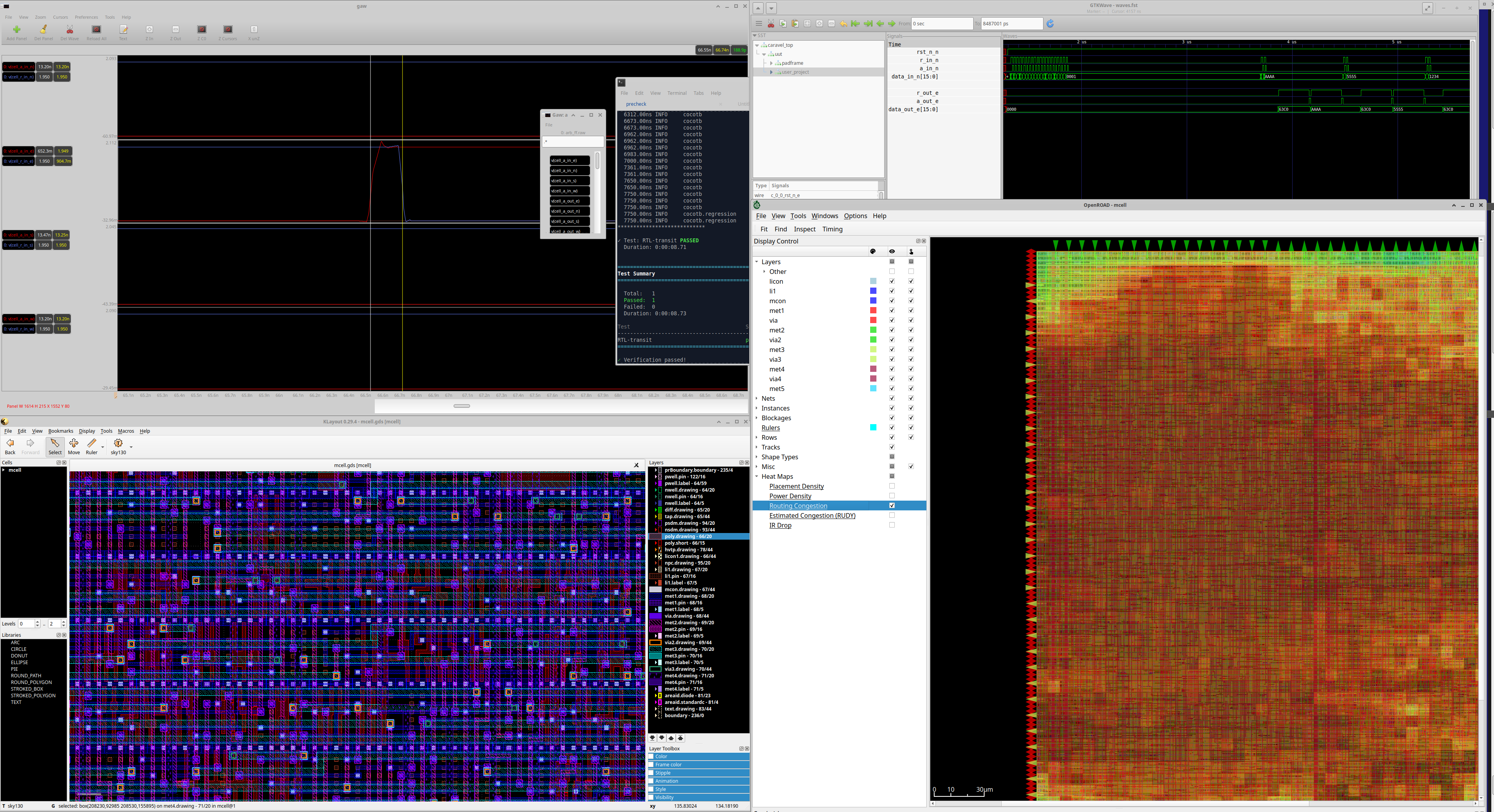
OpenROAD — Place and Route. OpenROAD takes the synthesized netlist and turns it into physical geometry. It places every cell on the die, routes metal interconnect between them, inserts fill, and generates a layout that satisfies timing, area, and DRC constraints. This is the tool that turns an abstract netlist into something that can actually be manufactured.
Magic — Layout, DRC, and Extraction. Magic is a venerable layout editor dating back to the 1980s at UC Berkeley. In this flow, it serves multiple roles: custom cell layout for our analog cells (C-elements, mutex cells, delay elements), design rule checking against the SKY130 rules, and parasitic extraction for post-layout simulation. It reads and writes GDS and integrates directly with the SKY130 technology files.
KLayout — GDS Viewing and Editing. KLayout is a high-performance GDS viewer and editor. We use it to visually inspect layouts, verify cell placement, debug routing issues, and perform final GDS manipulation before tapeout. When you need to look at what the tools actually produced, this is where you look.
xschem — Schematic Capture. For our custom analog cells—the C-elements, mutex arbiters, and delay cells that make asynchronous logic work—we draw transistor-level schematics in xschem using SKY130 primitive devices. These schematics feed into SPICE simulation for timing verification and into Magic for physical layout.
ngspice — SPICE Simulation. ngspice handles transistor-level analog simulation. We use it to characterize our custom cells: measure propagation delay, verify setup/hold times, check behavior across process-voltage-temperature (PVT) corners, and generate the timing data that feeds back into the digital flow. For an asynchronous design where timing margins are everything, SPICE verification is non-negotiable.
Netgen — LVS Verification. Netgen performs layout-versus-schematic checking. It takes the netlist extracted from Magic's layout and compares it to the schematic netlist from xschem, verifying that the physical layout actually implements the intended circuit. A clean LVS is required before tapeout.
Icarus Verilog (iverilog) — RTL Simulation. iverilog is our primary Verilog simulator for functional verification. It compiles Verilog source into a simulation executable that we run against testbenches to verify correct behavior at the RTL level, before synthesis. It handles behavioral, gate-level, and structural simulation and outputs VCD waveforms for analysis.
CVC — SDF Gate-Level Simulation. CVC is a compiled Verilog simulator optimized for gate-level simulation with timing. After place and route, the tools generate an SDF (Standard Delay Format) file containing the actual wire and gate delays from the physical layout. CVC performs gate-level simulation with these real delays back-annotated onto the netlist, verifying that the design functions correctly with actual silicon timing—not just ideal zero-delay simulation. This is the closest you get to testing real silicon before fabrication.
GTKWave — Waveform Viewer. GTKWave displays the VCD waveform files generated by iverilog and CVC. It is how you actually see what your design is doing—trace signals, debug timing, verify handshake protocols. For async design, waveform analysis is a primary debugging tool.
OpenLane — Flow Orchestration. OpenLane ties all of the above together. It wraps Yosys, OpenROAD, Magic, and the verification tools into an automated RTL-to-GDSII flow. You write a configuration file describing your design parameters—die area, target density, clock constraints (or lack thereof, in our case)—and OpenLane runs the full sequence: synthesis, floorplanning, placement, clock tree synthesis, routing, parasitic extraction, timing analysis, DRC, LVS, and GDS generation. One command, full flow.
The PDK: SKY130
All of these tools are useless without a process design kit. The SKY130 PDK, released by SkyWater Technology and Google in 2020, is the first production-quality open-source PDK. It describes the SkyWater 130nm CMOS process: transistor models, standard cell libraries, design rules, metal stack definitions, and everything else needed to design a chip that can actually be manufactured.
The standard cell library we use is sky130_fd_sc_hd—the high-density library. It provides the basic digital gates (AND, OR, INV, MUX, flip-flops, buffers) that Yosys maps our RTL onto. For our custom asynchronous cells, we design at the transistor level using sky130_fd_pr primitives and characterize them to generate Liberty timing models compatible with the digital flow.
The entire PDK, including SPICE models, DRC rules, LVS setup files, and technology definitions, is freely available and pre-installed in the iic-osic-tools Docker container. One docker pull and you have a complete chip design environment.
The Platform: ChipFoundry ChipIgnite
Tools and a PDK get you to a GDS file. Getting from GDS to actual silicon requires a manufacturing partner. This is where ChipFoundry comes in.
ChipFoundry's ChipIgnite program wraps the entire open-source flow into an accessible platform. They handle the shuttle coordination with SkyWater, the Caravel harness integration (which provides pad ring, power management, and a RISC-V management core), packaging, and delivery. You submit your design, they handle the rest.
The result: roughly $15,000 gets you ~100 packaged chips on a production 130nm process. Your design occupies approximately 10mm² of user area inside the Caravel harness. From tapeout submission to chips in hand is approximately six months.
Why This Matters
The traditional path to custom silicon requires $100K–$500K in annual EDA license fees before you write a single line of Verilog. That is a barrier that kills hardware startups before they start. It means that only well-funded companies or universities with institutional licenses can do chip design.
The open-source flow eliminates that barrier entirely. A bootstrapped startup with no outside funding can go from an idea to chips in hand in under a year for the cost of a used car. The tools are mature, the PDK is production-proven, and the manufacturing path is established.
What was once a dream is now a reality. Companies can focus on chip development and not worry about tooling and licenses.
We are proof of that. Lattrex is a one-person company building a novel processor architecture on this flow. In the coming weeks, we will go deeper into each stage of the process and share how we adapted these tools for our fully asynchronous design—a design that has no clock, uses C-elements and mutex arbiters instead of flip-flops, and required custom characterization at every step.
Stay tuned.